PCB ASSEMBLY
keywords: PCB China, PCB assembly, PCB assembly China, China PCB manufacturer
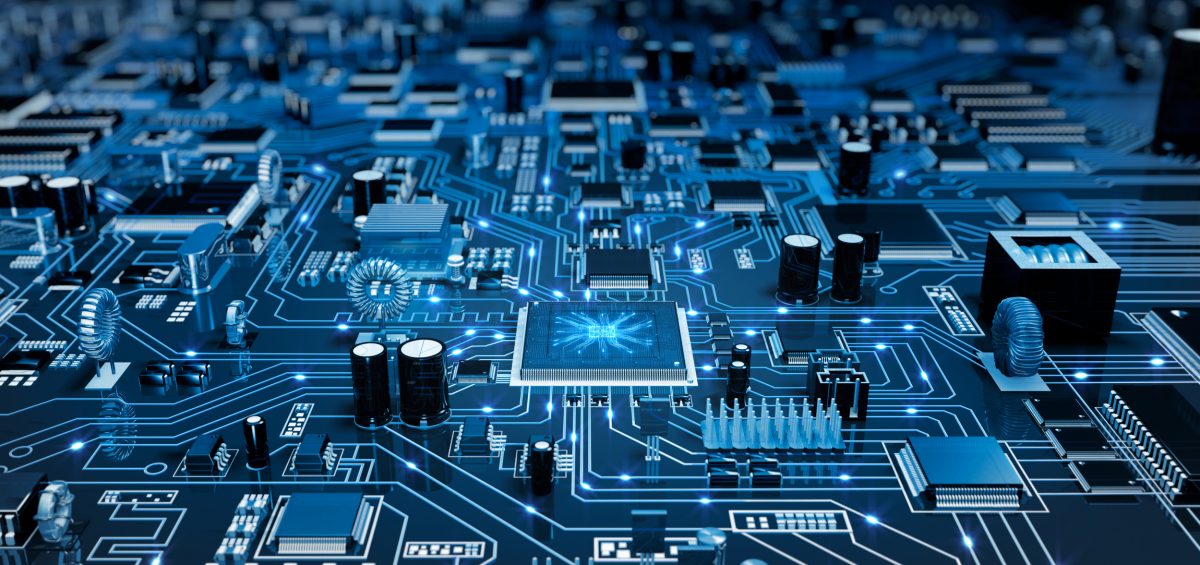
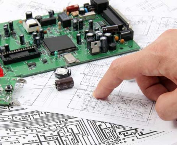
Simply put, a Printed Circuit Board or PCB, as it is more commonly known, is a thin board made of fiberglass or paper reinforced phenolic resin, and is further strengthened by copper foils. Electrical wires are, in a manner of speaking, ‘printed’ onto the board. This method of PCB assembly is a result of several decades’ worth of experiments, and many trials and failures. PCB assembly is one main part of electronic manufacturing services.
A PCB is generally used to support mechanically the pathways that are etched onto the board, and conduct electricity through them. In order to assemble a Printed Circuit Board, there is an assembled process that is maintained, and each step is carefully curated, so as to prevent as many error from human hands as possible.
A Printed Circuit Board is made via a PCB assembly, with a number of manufacturing processes, divided into several stages. However, all the processes from the PCB assembly come together in the end, to form an integrated and well-oiled final product. It is necessary for every stage of production in the PCB assembly to be congruent with the succeeding stage, as a clear and transparent mode of production will ensure that all problems that are detected will be solved in an easy manner, without stopping or delaying the advancements in the manufacture of other products in the PCB assembly line.
Breaking down the PCB Assembly Process
The PCB manufacturing and assembly process consists of many varied separate stages, beginning with choosing the right base for the main framework. Most Printed Circuit Boards are composed of copper, as the metal is well known for conducting electricity in a safe manner, without heating itself. Once the base is set and prepared, the other stages include:
Adding solder paste: Solder Paste is made from powder metal solder, mixed with a medium called Flux. This forms a grey gooey paste, which is then used to hold the various parts of the PCB together, till they can be definitely soldered. Typically, solder paste is added to components that are being melded, and this method is fulfilled by using a Solder Screen, one of the most important parts of the PCB assembly process.
Solder Screen: The solder screen is one of the most important aspects of this entire process of manufacturing a PCB assembly line. The screen is used to accurately sublimate the perfect amount of solder paste. This process is usually achieved by screen printing the solder paste through a stencil, but lately, jet printing is also being used as a cost and time saving mechanism. This process is extremely important, because if the adding of the solder paste is not done in a proper manner, there can be huge losses and widespread defects in the PCB assembly line currently being manufactured.
In recent times, the most common method of applying solder paste is through squeegee blade printing. The squeegees refer to the tools that are utilized to move the pasty solder paste from the stencil, and on to the Printed Circuit Board. The tips of the squeegee blades are usually made of rubber, to wipe off any excess paste. The metal of the blades has now been advanced enough to use polyurethane.
Pick and Place: In this part of the PCB assembly process, the board, with the basic structure all ready, is passed onto the Pick and Place machine. Here, an apparatus that is filled with various components for different Printing Circuit Boards ‘picks’ the components that it feels are the perfect fit for a particular PCB, and ‘places’ them on the correct positions on the board. The machine tends to pick up the placements of the components through the silk sheets that are ‘printed’ onto the board. Till the board is transferred to the next process of production, the components are held together by nothing but the tension on the solder paste. However, this is barely enough to keep the components immovable on the board. Sometimes, the machine places small droplets of glue to secure the board. However, this is only done if the board is to be wave soldered, as in that process, the droplets of glue gradually wear off and disintegrate.
Previously, the Pick and Place process was done by hand. However, hand processed PCB assembly is more prone to fallacies, which may lead to incorrect part placements and in some cases, the destruction of the entire PCB assembly line. Soldering by hand is also disadvantageous, as the process takes much longer to complete by hand. Additionally, the solder paste is also not spread as evenly and as widespread as compared to soldering with a machine.
Soldering: Soldering is a process by which two metals are joined together and melted, and then a second liquid metal is poured on top of it, filling any gaps that form. A solder can be best described as a metallic glue, which is used to maintain current flow and also hold the different components together. The main point of soldering is that the joining metal should be of a lower melting point than the metals that are being combined together. This is essential because only the solder needs to melt, not the parts that are being soldered. This helps in the solder liquid being able to reach the gaps between the two components easily, and can fill the spaces between them.
Wave Soldering, another time saving and distinct method used in the production of the Printed Circuit Board assembly line, is a process by which the Circuit Boards are filled with the solder metal to glue the different components of the board together. A tank like container holds a large quantity of the metal, and the board is passed from under it, and the metal is poured on it, just like a waterfall. The meal goes inside gaps and spaces between the different components, and the glue that is stuck in between the various parts of the Circuit Board are also dissolved at this time, and wear off. However, this method of soldering is also not without its disadvantages. There is a high chance that the soldering liquid may not go all the way through and reach every component on the board, and this might result in problems like cracked joints, poor hole fills, solder skips, and mask discoloration.
Inspection: After the process of soldering is over, the boards are always inspected for quality purposes. This process is always undertaken by an automated optical inspection, a process by which a camera scans the board through and through, in order to check for manufacturing defects like a ‘catastrophic failure’, which is caused by missing components on the board, and ‘quality defects’, which is a term that is applied when a component in the Circuit Board festers up, or when there are discrepancies in the fillet size and shape. This method of scanning by the camera can be used in many various stages, for example when the bare board is being constructed, or when the solder paste is being filled, and even before or after the solder liquid is poured into the Circuit Board. However, the automated optical inspection always takes place after the solder liquid has been filled into the board, as in the inspection can take place in one place at one time, and all the different aspects of the PCB can be inspected together. If a problem is found in any board during the time of the inspection, the board is promptly removed from the PCB assembly line, and if it can be fixed, it is attended to, otherwise it is discarded. The other boards that pass the inspection stage, are sent onwards towards the next production process.
Test: Before leaving the warehouse, all the Printed Circuit Boards have to be tested. There are various ways in which the PCBs are tested, including the Everett Charles ATG test,fixtureless testers, and the universal grid testing capability. However, some of the more popular methods that the boards are tested, are through Bare Board Testing, and Resistance Testing.
In Bare Board Testing, the capacity for a board is tested by introducing ‘shocks’ onto the circuit board, to measure the capability of the board. Discrepancies are formed due to natural variations in the build of the circuit boards.
Resistance Testing determines the amount of electricity surcharge that a board can handle. This too, falls prey to the inherent differences that come with each Circuit Board.
Feedback: It is the responsibility of the company that manufactures the Printing Board Circuits to also monitor the outputs regularly, and make sure that all their Circuit Boards perform satisfactorily in the real world. If any failures are detected, it is the responsibility of the company to investigate into the mistakes that were made, and try to improve on bettering the quality of their products, so that the past mistakes are not repeated in the future. If the manufacturers continue to assess the feedback that their produced boards receive in a regular manner, then they can also make sure that if a board has gone out with potential life threatening consequences, they can stop the PCB assembly production line, and rectify the issue, before it gets too late.


8 comments