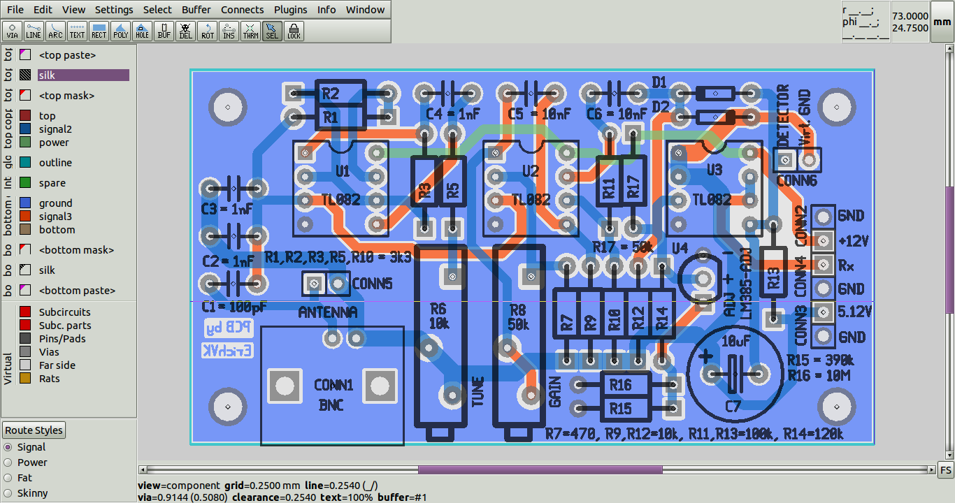
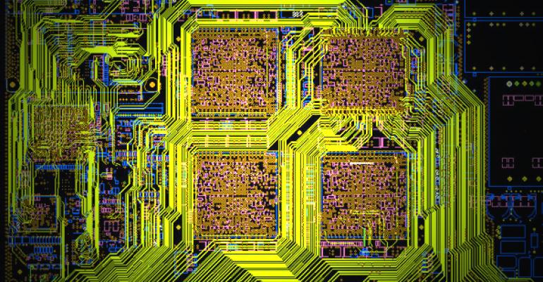
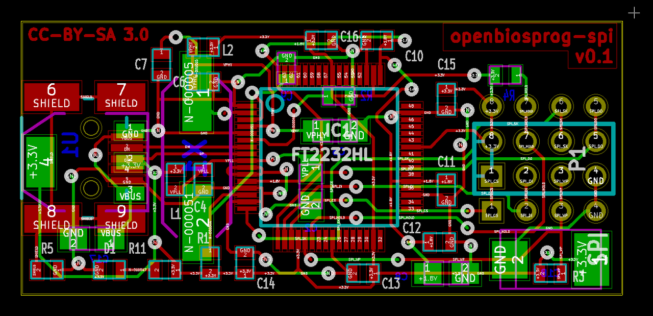
Printed circuit board (PCB) design and layout is both an art and a science, requiring a strategic consideration about the prime space available on your board. Creating a reliable, functional, yet cost-effective circuit and finished PCB can be a challenging task, especially in today’s demand for increasingly-complex requirements for compact, light-weight, even flexible boards.
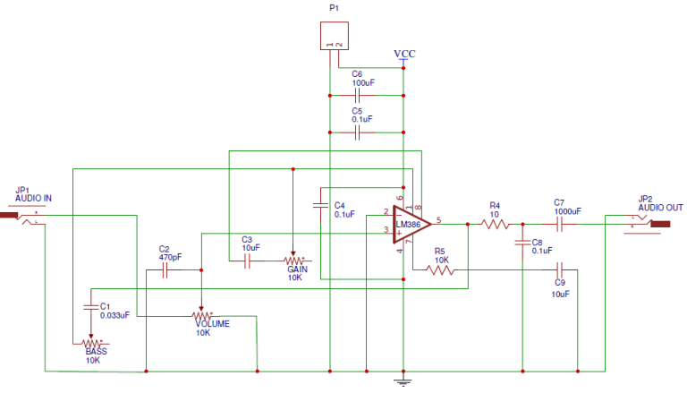
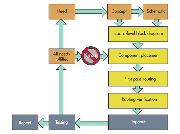
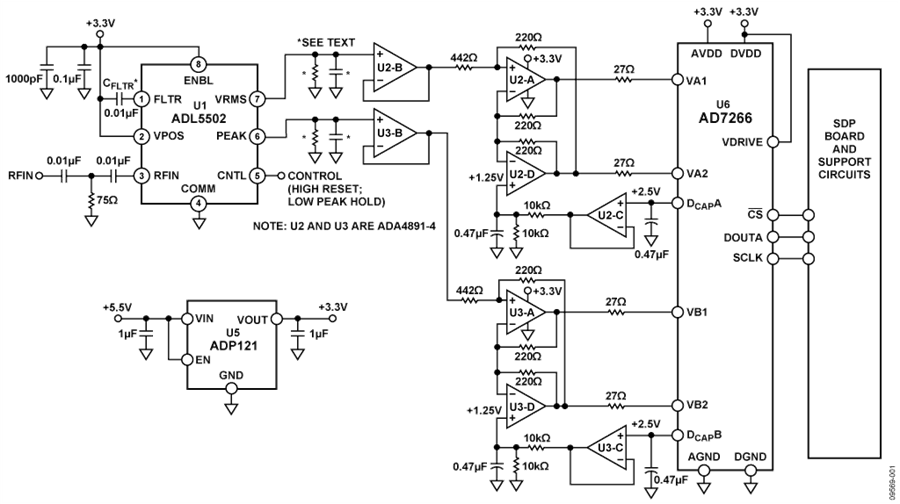
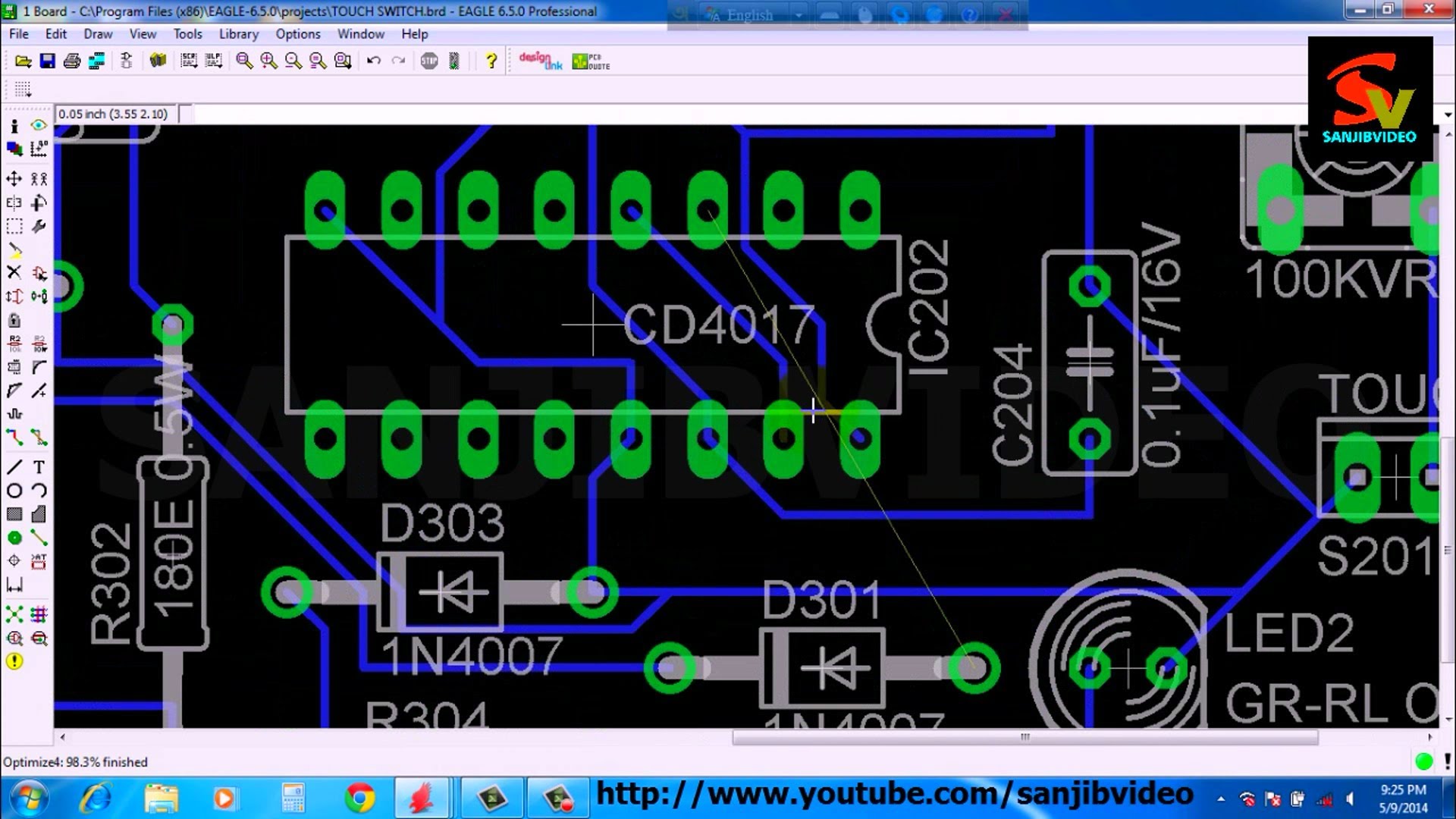
The design flow of PCB always starts with a schematic, followed by component placement, routing signal trace, and finishes with Design Rules Check and Gerber files generation, which is explained accordingly below with each tab.


