Film Generation
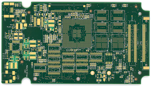
The film is generated from the design files (Gerber files), which are sent to the manufacturing house where each film is generated per layer.
Inner Layer Processing
This step includes cutting raw materials, roller coating, exposure, DES line and hole formation. The core of the layer is a panel of laminate, also known as substrate material, which provides a core strength to the PCB and helps resist breakage.
Mass Lamination
Laminating the PCB Layers is basically applying laminate between the layers which are aligned and layered up, where laminate is an epoxy resin and glass-fibre core with copper foil pre-bonded onto each side.
Drilling
This step is to use NC machines and carbide drills to drill holes according to the drill spec sent to the manufacturing house.
Copper Plating
The electroplating process fuses the different layers together using chemical deposition. After a thorough cleaning, the panel undergoes a series of chemical baths. Part of this bathing process coats the panel in a micron-thick layer of copper, which is deposited over the top-most layer and into the holes that have just been drilled.
Outer Layer Processing
In this step, we are imaging and plating the outer layer. A plating of tin beforehand is to help protecting the copper of the outside layer during the etching process.
Solder Mask Application
In this step we apply solder mask area to entire board with the exception of
solder pads.
Silkscreen
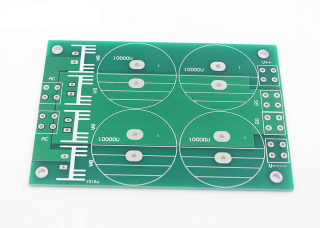
Apply white letter marking using screen printing process, used to indicate all vital information pertaining to the PCB.
Electrical Test and Final Quality Control
In the last step a technician will perform electrical tests on the PCB which
confirms the functionality of the PCB and its conformity to the original design.


