Article Outline
Chapter 1
What to Know About PCB Fabrication
Chapter 2
How is PCB manufactured?
Chapter 3
The best outsourcing option for PCB manufacturing

Chapter 4
PCB Prototyping Process
Chapter 5
How to Choose a PCB Prototype Manufacturer

Chapter 6
Conclusion

1. What to Know About PCB Fabrication
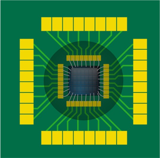
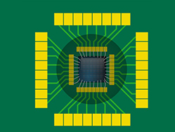
Print circuit boards can be found in almost every electrical products specifically on gadgets that you can probably think of. The print circuit boards have components which are arranged and gathered to make a circuit for an electric device. Therefore, PCB’s normally functions as the central command or the electronic devices’ command center.
The function and essentiality of PCB on any electronic devices didn’t achieve much of the spark not till the mid-1950s. Furthermore, it had a been a game-turning development of PCB on any electronic devices, coming from a point on point construction anionic and wire wrap the spark of PCB has allowed electronic and mechanical devices to be much small in size.
In today’s era, the world is becoming more and more dependent on electronic and digital devices, and as it dramatically increases, demands on PCB are highly expected to grow further in the following years. Currently, PCB’s always amazed us by getting smaller, but besides that, it can do more than what it does.
In this selection, we will tackle the basic prototyping of PCB plus the preparation needed before its prototyping procedure begins; it includes the known PCB fabrication specs and PCB design software. We would also tackle the disadvantages and advantages of outsourcing and in-house PCB prototyping. Far along the article, you’ll be able to have knowledge on this step-by-step process of prototyping a PCB and on how to correctly choose the best manufacturer of PCB prototype.
1.1 PCB Assembly Vs.PCB Fabrication
Before we start to dig deeper with the processes of PCB prototyping, let us first clarify the terms that are commonly interchanged and often misused in the world of circuit board manufacturing- PCB Assembly Vs.PCB Fabrication (PCBA).
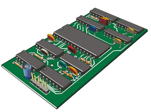
PCB Fabrication
implies the making of printed circuit boards.
Upon the other hand.
PCB Assembly
involves the fusing of the components unto the boards wherein it could both be through-hole or surface-mounted.
1.2 Kinds of PCBs
Printed circuit boards are made into three various types such are, double-sided, single-sided, and the multiplayer. The complexity, functionality, and size of the design of your printed circuit board highly determine the amounts of layers appropriate in a committee.
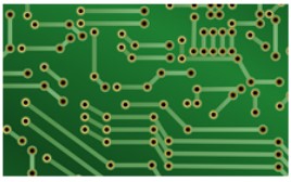
1.2.1 The single-sided printed circuit board
Printed circuit boards are made into three various types such are, double-sided, single-sided, and the multiplayer. The complexity, functionality, and size of the design of your printed circuit board highly determine the amounts of layers appropriate in a committee.
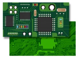
1.2.2 Double-sided printed circuit boards
Printed circuit boards that are double-sided are considered to have more complexity if compared to the single-sided PCBs because the number of the components or the circuits cannot easily on only one surface of the substrate. Hence, it usually consumes two-sides of it.
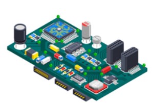
1.2.3. Multilayer printed circuit board.
These kinds of printed circuit boards are known to be the most complicated among the three PCBs given its name “Multilayer,” it is comprised of plenty layers on which circuits are linked through drilled holes and wires.
2. What is Printed Circuit Board Prototyping?
- 2.1 Advantage of PCB Prototype
- 2.1.1 Capability to discern Flaws
- 2.1.2 Capability to Analyze Every Component
- 2.1.3 The Streamlined Workflow
- 2.1.4 The Cost Reduction
- 2.1.5 Illustration of Finishing PCB
- 2.2 Options on PCB Prototype
- 2.2.1 The Visual Model
- 2.2.2 The Concept Proof
- 2.2.3 The Working Prototype
- 2.2.4 The Functional Prototype
- 2.3 Outsourced PCB Prototype and In-House PCB Prototype
- 2.3.1 Advantages and Disadvantages of In-House PCB Prototype
- 2.3.2 Advantages and Disadvantages of Outsourced PCB Prototype
- 2.4 China’s PCB Prototyping
Ever since the beginning of this lecture we talked about PCB prototyping. the question will be: what is PCB proto-typing? Where does the PCB prototyping apt in all these? Now is the time to dig deeper. Before a specific printed circuit prototype board set out to be mass produced in the market. it will first go through the manufacturing process of a printed circuit board prototyping most of the moment.
The prototyping of PCBs can be of greater use throughout the circuit board manufacturing process of printed circuit boards. for the reason that it’s where you usually check and tests several aspects of designs ahead of producing it to the market.
Consequently, PCB prototyping had been a time-consuming. and tedious process. mainly if there exist many revisions brought about by complexities regarding the printed circuit prototype board. Therefore. it is practical. To begin with, a low-cost way to make each PCB prototypes.
Before buying or ordering a printed circuit prototype board, you will need to be sure that a particular prototype fabrication store or the manufacturer of a PCB prototype can efficiently meet your demands. You will find out more about getting to choose the best manufacturer of PCBs under Chapter 5.
And before we dig considerably into the processes of printed circuit proto- typing boards. it is much recommended to manage the goals you set for your PCB board from functionality and appearance.
The target of the PCB prototype basing on the appearance, otherwise known as the look-like model, is mainly to stay focus at the aesthetics or physical form of the PCB prototype board. The techniques of PCB prototyping are clay or foam 3D printing. injection molding, and CNC machining. On the other hand, the aim of a printed circuit board prototype if base into its usage is to sort out any possible technical difficulties.
2.1. Advantages of PCB prototyping
Usually, PCB prototyping is much prescribed if the printed circuit prototype beam will be further used for several products which are set to access the market. It explains why PCB prototyping does beneficial and essential for many purposes.
 2.1.1 Capability to discern Flaws
The primary reason why the prototyping of PCB occurs is to spot flaws in the design of your PCB. And instead of directly going to a conventional PCB production. the printed circuit board can provide you a possibility to examine your PCB prototype board for some defects and to solve these problems before producing it to the market.
Because if a sophisticated design that left unreviewed be mass-produced in the market. it would move a whole lot of cents and efforts into waste.
 2.1.2 Capability to analyze Every Component
For PCB prototype boards that have intricate designs, it would be practical to check and question out all the components of a PCB step-by—step to be sure that they do functions well. You will need to verify if the PCB prototype board can withstand a particular condition, such includes the variations of power. Shock resistivity. and changes on temperature. if not. It will be way much tricky to spot the problem once the PCB prototype board is assembled and ?nished.
 2.1.3 The Streamlined Workflow
If you can discern flaws and examine all the components or circuits of a PCB prototype board. then it would make your workflow beyond efficient. And through that. you would get a more signi?cant chance to get your timelines accurate.
 2.1.4 The Cost Reduction
The PCB prototyping would not only result in a productive workflow; however, it can also boost the happiness and satisfaction of your bottom formation. By acquiring a PCB prototype board, you will more likely reduce the price brought about by needless mistakes in production. irrespective with the amount of run on your PCB production.
 2.1.5 Illustration of Immediate PCB
Acquiring some information on how the standard PCB you have performs when it’s incomplete swing is very necessary. And it would only be through the use of a PCB prototype board where you can measure the accurate size. Performance, composition, etc. of your of?cial PCB. Still, with the existence of tolerances within PCB prototype boards. you will be able to fetch ideas on what an already done PCB board would look like and on how it will work.
2.2 Printed Circuit Boards Prototype Boards
There are many types of PCB prototypes, plus each varies largely in usage within the levels or degree of the process on prototyping a PCB. It mainly hinges on anything you would want to make use of in a PCB prototype or rather what you are looking for in a PCB prototype, the manufacturer of your PCB prototype might suggest the use of not just a single PCB prototype yet more than two or even all of the PCB prototype they have.
2.2.1 The Visual Model
The Visual model of a printed circuit board is operated to show the whole visible structure of your coveted PCB design also to imitate the actual standard printed circuit board. Electronically. the visual model doesn’t only work as this is an intended usage to review and demonstrate the design of a PCB in a very reasonable way possible.
2.2.2 The Concept Proof
The Proof of concept (POC) is the type of prototype that displays the practicality of the design from your PCB. However, not the whole skills of the conventional printed circuit board are incorporated. but it’s sufficient to show if your PCB design is probable.
2.2.3 The Working Prototype
The working prototype works the same as the standard PCB; however, it‘s not quite just as much as it is. It has every function that is planned intended toward the last board. However, these may be directed to alterations before getting a run on being mass produced.
2.2.4 The Functional Prototype
The functional prototypes are primarily designed to be equally comparable with the standard printed circuit board. It must include entirely the capabilities and characteristics intended only for the last and end PCB, which indicates it should reach the production-quality then.
2.3 Outsourced PCB Prototype Vs. In-House PCB Prototype

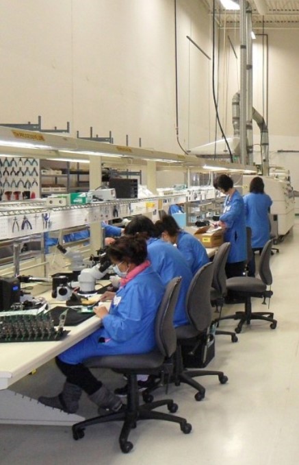
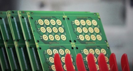
The duration it would take to make a brand-new product starting from only a design until the stage of PCB manufacturing is of immense importance in the current on-demand society. And this resonates mainly on the design aspect.
Usually, a particular model is devised, and then the construction of the PCB prototyping is subcontracted to a linked third-party, frequently based abroad. Regardless, there are many factors concerned that need to be considered when operating an outsourced PCB prototyping preferentially an in-house prototyping industry.
2.3.1 Advantages and Disadvantages of In-House PCB Prototype
Printed Circuit Board (PCB) is undeniably time-consuming. And time is the main driving advantage you can get from performing in-house prototyping of PCB.
And if your set timeline is designed to be stern, you might need to consider switching to the process of an in-house PCB prototype. The in-house prototyping process gives you the capability to accelerate your construction of a PCB prototype of weeks or months into just only a count of hours and even minutes.
Maintaining the process of your PCB in-house would also signify that valuable designs can be contained just inside your corners. That could protect them from a third-party to be involved such as manufacturers of PCB prototype because it can prevent them from spreading, leaking, or copying the PCB design you made.
Nevertheless, PCB prototyping continues the kind of process that mainly requires a constant change, regeneration, and redesign. Executing a method of an in-house PCB prototype would signify you’ll be carving free from PCB prototype manufacturers, that significantly implies you will have to do it at your own, and on the best way, you can.
For this procedure to be as easy as it can be, your line of in-house PCB prototype should be adaptable and flexible to immediate changes in your design or an abrupt addition of further parts as well as to the direst scenario wherein you would’ve needed to restart this prototyping run on your PCB.
2.3.2 Advantages and Disadvantages of Outsourced PCB Prototype
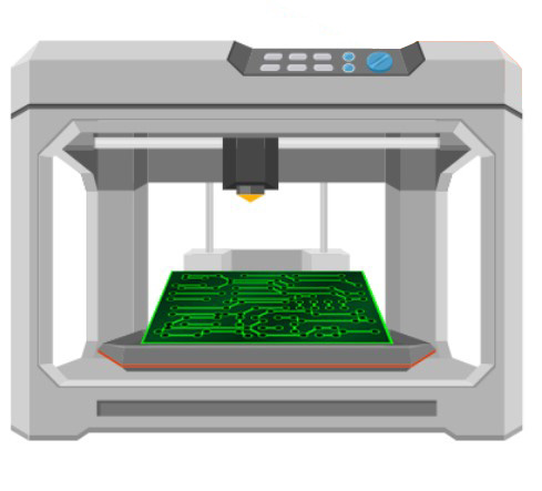 The outsourced PCB prototyping, on another hand, is enormously cost-efficient, much especially to a manufacturer of PCB prototype that is located abroad. However, more than what is apparent savings on the price, outsourcing PCB prototype accepts the distribution of more hypotheses, tests, and ideas toward your project.
From their own experience, the manufacturers who are the third-party in making a PCB prototype can arise with various testing experiments, cycles and new item schemes that you may not have conceived of or utilized before.
Unfortunately, the inspection part is a difficult task in the process if you decide to outsource the printed circuit board prototyping procedure overseas. Moreover, outsourcing this PCB
prototyping procedure, especially through abroad, can place a hindrance toward your overall method whenever your PCB prototype board is muddled up.
2.4 Prototyping of PCB within China
 Outsourcing product manufacturing from PCB manufacturing companies within China has been the standard routine for many corporations and companies throughout the world. However, the outsourcing regarding printed circuit boards prototyping within China as well as prototyping, in a general discussion, is still within its early stage; and it is not as much common compared to mass production.
Just as much as all business verdicts, outsourcing of PCB prototypes through a China PCB manufacturer has its particular set of pros and cons, and the distinct style for the drawback to overshadow the advantages is to consider your wants or your goals well and to take the more appropriate steps. Additionally, if you would want to know more about getting your proper pick of a printed circuit board prototype manufacturer, browse our comprehensive guide discussed into Chapter #5.
China performs as the most excellent country to get your standard PCB or PCB prototype to be manufactured because it’s a justly affordable country to assemble, even for low volumes and prototypes. Companies that are based in the United Kingdom, the United States, or Canada, and elsewhere in the world can probably reduce their charges on PCB prototyping. It can be accomplished by taking full advantage on the scale of economies that would have been created to assist the immense number of development in hardware that is holding the place in the specific country, specifically in Shenzhen, which is the electronics hub of the entire world.
Making a statement about how China is some low-quality, the low-cost market has, at some degree, turn out to be a statement in the past. Because in reality, China had disbursed $1.1 billion at preservative manufacturing during the year 2017, which typically means that its market in prototyping is growing exponentially.
Cost savings and cost reduction are the primary reasons why corporations and companies come to a China PCB manufacturer for their needs in PCB prototyping, which makes this a market with extraordinary value. Nevertheless, this low-value seldom happens with the cost of quality, that is why you should be cautious of what you would be dealing with.
Additionally, logistics are still the primary concern why outsourcing a prototyped PCB in China is considered as a significant disadvantage. Correspondingly, the security of trademarks, trade secrets, patents, and copyrights are a considerable concern as well, because it’s not only about outsourcing within China but also working beyond borders between countries and such because there will always be language and cultural problems.
On the other hand, beside this ever-growing business of circuit board manufacturing in China, this shouldn’t be hard to seek the exact manufacturer of PCB prototypes that could accommodate your prototyping demands and such with your printed circuit board.

3. Preparing for PCB Prototyping Process
- 3.1 The Gerber Files
- 3.2 The KnownPCB Design Software
- 3.2.1 The Eagle
- 3.2.2 The OrCAD
- 3.2.3 The KiCAD
- 3.2.4 The Altium Designer
- 3.2.5 The PCB Wizard 3
- 3.3 The PCB Fabrication Specifications
- 3.3.1 The Dimension
- 3.3.2 Amount of Layer
- 3.3.3 The Material
- 3.3.4 The Board Thickness
- 3.3.5 The Pad Plating
- 3.3.6 The Impedance Control
- 3.3.7The Minimum Spacing/Width
- 3.3.8 The Hole Sizes
- 3.3.9The Solder Mask
- 3.3.10 The Silkscreen
- 3.3.11 The Minimum Pitch
- 3.3.12 The Castellated Holes
- 3.3.13 The RoHS Compliance
After having learned all the needed basics of prototyping a PCB and as well as its advantages, it’s now time to outlay the base for the process of PCB prototyping. Within this section, we would walk you withain preparation before we jump into the prototyping process of PCB. You will know and hopefully familiarize the specifications on PCB fabrication, few of the standard design software of PCB, and what Gerber files are.
 3.1 The Gerber Files
The Gerber files remain known to be the digital outlines that let your manufacturer of PCB prototype or a manufacturer of PCB make your PCB cover by cover. Numerous premium, as well as free PCB software designs, have a built-in tool in generating the Gerber files, so as OrCAD, Eagle, Altium Designer, KiCAD, and more. You would know further about this software for PCB designs in the preceding segment.
 3.2 The Known PCB Design Software
The PCB prototype or PCB would be nothing without software for PCB design. The level of achievement of your printed circuit board prototype in some way depends upon your selected PCB design software and on how you utilize it.
It’s not always a simple task to pick which PCB layout software, so in that section, we wish to acquaint you to the commonly preferred PCB design software accessible at the store today, both the premium and free-to-use loads.
3.2.1 The Eagle
The Eagle belongs to the few most known software of PCB designs out there in the market, and that is because it is user-friendly and free-to-use. The Eagle’s free version lets you use two signal covers, 80cm² board space, and two schematic sheets. If you would be inconsequent need of more, you’ll be able to upgrade into the premium plan, but still, since its a premium package, it’s at a portion of mostly PCB design software’s cost.
The drawback of this kind of PCB design software is its lacking high-end attributes that allow users to make a simple outlay of routing features or other signal designs that are high-speed, an example of these were pushed shove routing. Moreover, its overall workflow on the plan is slightly dated. However, generally, Eagle is way more of a prominent option for advanced users and especially the beginners as well because they would not need to do more complicated designs.
Eagle is free and can be downloaded on Linux, Mac, and Windows.

3.2.2 The OrCAD
The OrCAD is among the few newly launched professional level software PCB designing. It mainly offers each of the high-end qualities and skills you’ll need, which includes the group routing, 3D modeling, advanced auto-router, curved routing, and DFM checking.
The quantity of the design analysis and signal tools turn it to be very handy for roughly all your prototyping needs for your PCB. It likewise has several trim levels, which includes its free version, and that is OrCAD Lite. Sadly, it is comprised of a steep education curve which further explains why beginners might notice this challenging to operate at the start.
OrCAD is downloadable and is available on MacOS, Linux, and Windows.

3.2.3 the KiCAD
The KiCAD is an open-source software on PCB designing, which practically means that it’s free for use for anyone. It contains a schematic PCB, a component module and a high-end quality that could be found in a professional and standard PCB design software, such as, push shove routing, 3D modeling, hierarchical schematic design, and differential pair routing.
And because KiCAD is open-source software, it is made up of a vast community of its contributors and users that gives you the support on any of your concerns that are software-related. Nevertheless, it might be a little difficult to steer this software because of its irregular workflow and disorganized modules.
KiCAD can be downloaded and is available on MacOS, Linux, Ubuntu, and Windows.

3.2.4 The Altium Designer
The Altium Designer is among the known amateur PCB design software. And some of the main features involve a , 3D modeling, auto-router, PCB module, schematic, track breadth tuning and differential pair routing.
But unlike many professional level PCB design software, this Altium Designer is more straightforward to use. Nevertheless, its set of rich features and sheer price point might make DIY communities, and hobbyist next guesses.
Altium Designer is now available and can be downloaded on Windows.
3.2.5 The PCB Wizard 3
The PCB Wizard 3 remains a low-priced, easy-to-operate PCB design software which is as equally compelling as the suites that comprised of a high-end scheme. It permits you to make a single as well as double-sided prototype designs of PCB.
It is comprised of a PCB section placement, schematic capture section, auto-router, and board outline component. On top of these, the PCB wizard 3 lets you generate many types of bill of supplies report as well as modern file formats. Nevertheless, it doesn’t have a viewing feature that is quite an in-demand in the market which is three-dimensional.
PCB Wizard 3 is now available and can be downloaded on Windows.
3.3 The PCB Fabrication Specs
The PCB fabrication specs are scheme demands that have a significant influence on the cost of your product, yield, manufacturability, and supply chain. And failure to resolve PCB fabrication specifications might appear in a costly process of PCB prototyping (and the expected item) and an inexpensive yield.
To assist you in saving money and time in the process of prototyping a PCB, here are the fabrication specifications that you will need to absorb. Instill in mind that if compared to the standard PCB board the PCB prototypes vary a little in specs.

3.3.1 The Dimension
It merely is the actual measurement of your board. This mainly asks the question, how vast is your PCB prototype in scope?
The price of a particular prototype board of PCB is measured with its surface area, that’s why you will need to make sure that you only utilize the exact space you want to lower down your expense from it. Also note that the prototype designs of a PCB board with an irregular shape that usually results to waste materials through the fabrication of a PCB will charge you much more significant than a rectangular, and smaller trace for a comparable board.
On the other hand, for a prototype board of PCB, the maximum size of the board is 500mm x 500mm while the minimum size of the board is 10mm x 10mm. For a standard printed circuit board, the maximum size is 600mm x 700mm, and the minimum board size is 6mm x 6mm.
3.3.2 The Number of Layers
The count of layers within the prototype board of a PCB shows the stage of complexity this resides. The more copper layers there is in a PCB means the bigger chances of pins and components to go across and overlap one another. Usually, the prototype boards of a PCB has some 1-8 sheets, and the standard PCB has 1-32 leaves.

3.3.3 The Material
Two of the prevalepopularnt type of printed circuit board materials that are utilized nowadays are the phenolic paper, identified as the FR-2, and the fiberglass epoxy, defined as the FR-4. Other types of printed circuit boards that are less known materials include polyimide, Teflon, and peek ( or known as polyether ether ketone).
The Glass epoxy is usually the evading choice of almost all the prototype manufacturers of PCB, to which it has to be more cautiously planned of if ever your processes include RF boards or high-speed. The phenolic paper is way more harmful and tends to be prone to cracking and chipping.
3.3.4 The Board Thickness
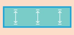
The thickness of the board is a significant mechanical specification on a PCB. The typical industry model for the width of a standard PCB is 0.4mm to 3.2mm while 0.4mm to 2.0mm for the PCB prototype board.
Nevertheless, the copper layers’ number indicates the main dimensions of a standard PCB and PCB prototype board basing on the level of thickness you desire. Tight and small PCB prototype boards might command for a 1.0mm depth more or less.
3.3.5 The Pad Plating
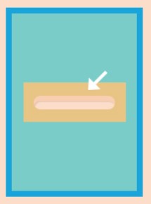
Pad plating remains the coating method of your PCB where the copper surface’s exterior within a standard PCB or a PCB prototype board is enclosed with an added metallic material. And this technique improves
the solderability regarding the pads significantly when assembling.
Two of the most popular plating methods for PCB prototype boards are either lead-free or led ENIG (electroless nickel immersion gold) and HASL (hot air solder leveling) plating. The latter have more endurance to flatness and oxidation, but it is more expensive, while the former uses solder within the board when assembling the PCBs.

3.3.6 The Impedance Control
For a standard PCB or a PCB prototype board that has an installed radio upon it, so as NFC, Bluetooth, and Wi-Fi, impedance control needs to be stated. Numerous factors affect the impedance; it includes the trace width, solder mask, and the prepreg material’s dielectric. For instance, the circuits of a Wi-Fi antenna are usually limited over 50-ohm impedance.
Impedance regulator can solely be controlled by costly equipment which cannot typically be found in any PCB prototype manufacturers’ services. And if it’s something you demand your PCB prototype board, you would need to add this service on the cost lists about your PCB fabrication.

3.3.7 The Minimum Spacing/Width
The minimum spacing/width is known as the actual distance between each copper traces within your standard PCB or PCB prototype board. Several manufacturers of PCB prototype can manage down to a 3-4 mil spacing, even though six mil spacing is equally safe. A PCB prototype board that possesses an appropriate spacing can move out 64 or 128 pins of a particular microcontroller, which is quite nifty.

3.3.8 The Hole Sizes
In stating the vias and the exact dimensions of the holes on your PCB prototype board is the best way to take full advantage of the space. The tolerance of the aspects of the holes on a prototype standard PCB and PCB board is ±0.08mm – ±0.15mm.
The less tolerance on the hole size the stronger your manufacturer of the PCB prototype had to go over in the drilling process. And missing an understanding of the hole size might mean a tune of wasted materials.

3.3.9 The Solder Mask
Solder masks are used on the copper traces of a standard PCB or PCB prototype board to stop fused bridges from causing and forming some short circuits.
The manufacturers of PCB prototypes have colors with a variety for you to choose from. White is difficult to keep up; Green is known to be cheap, and black eludes cosmetic defects.
3.3.10 Silkscreen
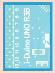
Silkscreens are the last layer within your standard board or PCB prototype board. It is comprised of graphics, the designators, and the text to assist in annotating your board.
This actual process is applicable called as the legend printing, but the silkscreen had become more known because it’s printing with an epoxy ink is the most known technique for marking the PCB legends. A more expensive version and a higher resolution of silkscreen printing example is the liquid photo imaging (LPI).

3.3.11 Minimum Pitch
Pitch is the space between nearby pins on a specific electrical component. Usually, the minimum size of a pitch is 0.3mm among the prototype manufacturers of a PCB. The standard PCBs and PCB prototype boards have a numerous pin that is adjacent to each other that is why having a moderate pitch requirement might yield more scuffle.
3.3.12 Castellated Holes
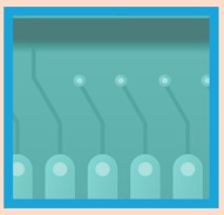
The Castellated holes are clearance and vias holes that are usually cut down in diameter to disclose copper alongside the face of the printed circuit board. Additionally, incorporating castellated pads to a PCB prototype board designs are highly recommended especially if your PCB or module mounts on another PCB. Not all prototype manufacturers of printed circuit boards can build PCBs that has castellated holes, that’s why you surely need to consider it.

3.3.13 RoHS Compliance
The RoHS stands for Restriction of Hazardous Substances Directive. The RoHS compliance is a critical concern that you will need to tackle with your PCB prototype manufacturer. The RoHS compliance mainly certifies that the product you made that is your product that is shipped and immediately sold to your consumers are free from toxic materials/substances and lead.
4. PCB Prototype Process
- 4.1 Design your PCB Prototype
- 4.2 Creating a Design Scheme
- 4.3 Creating Material Bills
- 4.4 PCB Routes Designs
- 4.5 PCB Prototype checking
- 4.6 Making Photo Film
- 4.7 Inner Layers Printing
- 4.8 The Aligning Layers
- 4.9 The Combining the Layers
- 4.10 Drilling the Holes
- 4.11 The Copper Plating
- 4.12 Imaging the Outer Layer
- 4.13 Tin Plating and Copper
- 4.14 The Final Etching
- 4.15 Applying the Solder Mask
- 4.16 Applying Surface Finish
- 4.17 Applying Silkscreen
- 4.18 Cutting the Board
- 4.19 Components Sourcing
- 4.20 Assembling a PCB Prototype
- 4.21 Stenciling a Solder Paste
- 4.22 Placing and Picking
- 4.23 Reflow Soldering
- 4.24 PCB Prototype Inspection
- 4.25 Through-Hole Components Insertion
- 4.26 The Functionality Testing
- 4.27 Testing PCB Prototype
- 4.19 Components Sourcing
When you have known all the fundamentals, you are wholly set to begin the prototyping process of a PCB. Numerous prototype manufacturers of PCBs can help you throughout the process. Working and associating with a prototype manufacturer of PCBs that offers a full turnkey of solutions can simplify the process because you would not need to deal with several companies back and forth in prototyping your PCBs.
Your finishing goal in prototyping is to reach a quality product PCB prototype that will work and look like your last, PCB prototype board to be mass-produced.
PCB prototyping is just about learning. And every time that you create a PCB prototype board, you would discover something new and fresh.
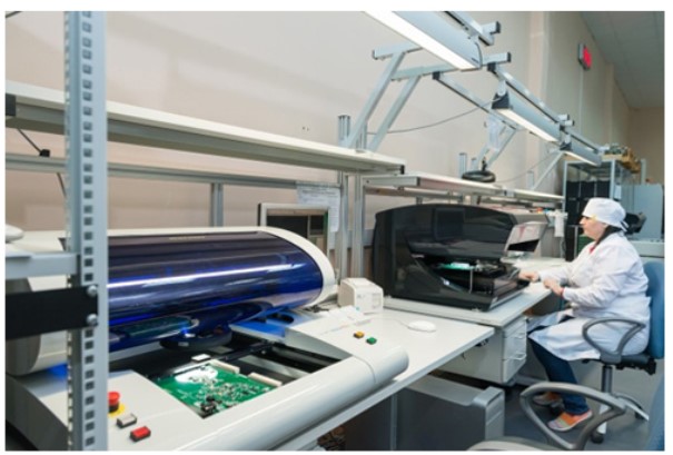
Start with the cheap and basic PCB prototype. And as you transform pieces and bits of the determined PCB prototype board, you will be capable of thinking up a PCB prototype design that is as equally best as the finished PCB prototype.
4.1 Designing your PCB Prototype
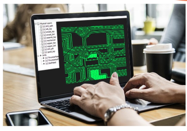
The design is the sole foundation of the prototyping process of a PCB. And as what we have said in the earlier section, you can take advantage of the premium and free PCB design software to arise with a PCB prototype design on your own.
It is highly recommended to begin designing a default PCB only if you are already convinced about the functionality of your PCB’s. And a default PCB prototype design can be convenient and practical to make before going into the mass production. Moreover, if you are considering creating a custom and default PCB prototype, you can always buy online because some perfboards and breadboards are available there.
The breadboards are solderless boards for temporary prototyping of PCBs. And it has some strips of metal beneath the board which interconnects the holes located at the top of the board. A perfboard on the other hand also called dot PCB, is another type of PCB prototyping material. Perfboard is a rigid, and thin piece with an already drilled holes at some standard intervals across its grid. It is generally created of paper that is laminated with a fiberglass epoxy or phenolic resin.
4.2 Creating a Design Scheme
AT the time you have already designed the PCB prototype, it’s the perfect time to arise with a design scheme, which then displays all of the project goals and requirements that PCB prototype engineers and manufacturers will utilize in the production process.
The schematic design may be comprised of info about components, hardware, and materials to be utilized in the PCB production. Additionally, it would also illustrate the function of the board, the array of the components, and characteristics. Moreover, agreeing on the best grid and panel size is efficient in this phase.
Generating a schematic design is not a one-time task. Because it still has to go through some preliminary checks to search out for possible mistakes and to rectify them.
After that phase, the scheme design needs to run on simulations with the use of a PCB design software to test if the PCB prototype works well. Note that once the replications are right, the schematic design on an electronic schematic design shall be formulated into a netlist, an account for the connectivity of the electronic circuit.
It assists in constantly running a rule checks on the design throughout the design process due to the opportunities it gives you to rectify the errors and defects as you go along.
4.3 Creating Bill of Materials
A bill of materials is typical to list each of the materials and components you will need for producing a prototype PCB board. And if ever you select to deal with a PCB prototype manufacturer, usually they will make use of this document to be sure if they have received the right ones.
A specified bill of materials might include the following info:
- The count of active components and materials.
- Designators of Reference are the codes that are used to familiarize each part.
- The specifications for every component and material that are displayed and described in the suitable units, such as farads and ohms.
- The footprint is the actual position of every component within the prototype PCB board.
- Manufacturer’s part number, it is the part number that is used by the manufacturer of the component.
When the schematic design bill and of materials are complete, a component engineer and an outline engineer shall check and collect these required materials and components. The component engineer is responsible for picking the materials and right parts that would work for the schematic design and will meet the size and price requirements of all the client.
4.4 PCB Route Designs
Outline PCB routing by linking the traces that are already on the board. And when you design the path of the PCB prototype, you will need to involve several factors like generating the signal noise, power levels, and noise sensitivity.
In most of the PCB design software, they have a netlist where you will need to create, and it would be utilized in planning the routing. Moreover, almost all of them can calculate automatically the most favored routes basing only on the number of available layers and such other factors.
If the PCB routing has become distressing to the point that many routes are crossing over each path, you need to consider making use of a double-layered PCB prototype board to make it all tidy and systematic. You will need to put one layer into the connections on the east-west part, and the other layer to the links on north-south.
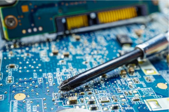
When designing a PCB routing, it can get plenty of time, especially if it’s a more complex and more significant prototype PCB boards.
4.5 PCB Prototype checking
Steering a daily rule checks on the design throughout the staging process can significantly enable you to push over issues with functionality before going into the stage wherein you are going to fabricate. And a full inspection is much recommended for you to check every piece of details on your design.
Thermal issues such as heat spots are one of the widespread problems you may run into. And it is required to maintain the temperature of your PCB prototype consistent. Inconsistent heat spots and temperatures are typically initiated by some features such as the size of PCB, thermal paths, varying copper thickness, and the number of PCB layers.
Aside from thermal checks and design rules, you also need to include some layout-versus-schematic (LVS) check, an electrical check (ERC), and an antenna check. And once these checks and the other quality assurance valuations are finished, you can continue to the following steps.
4.6 Making Photo Film
Handling your PCB prototype design, you or your PCB prototype manufacturer must a photo film about the prototype PCB board toward all layer including the solder mask of the board. The photo film comprises a plastic sheet marked with a photo image of the board, which indicates the conductive copper also non-conductive copper pieces of the board.
4.7 Inner Layers Printing
Copper will then be applied to a particular substrate material. And the prototype manufacturer of your PCB can do the job for you.
In this stage, the copper would already be mixed to the substrate afore putting on a sheet of photoresist. Then, it shall be exposed to ultraviolet light to toughen the photoresist further.
Areas that are blocked by clear ink coming from the schemer will stay melted or flexible. And then they would be detached the toughened photoresist afore.
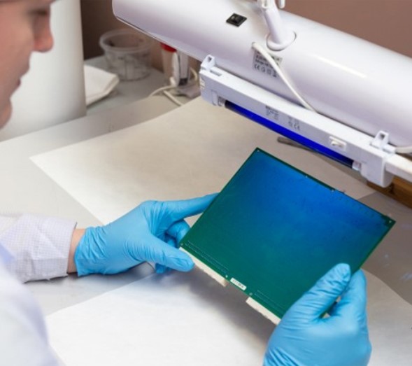
4.8 Aligning the Layers
For PCB prototypes that have multiple layers, you will need to arrange them and push specific registration gaps. The arrangement needs to be accurate. Otherwise, if you would combine the layers with the layers inside, they will match.
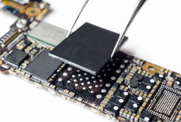
4.9 Combining the Layers
The outside layer of the materials are named as a prepreg, and the original substrate is wrapped by a copper foil which contains a combination of copper trace etchings.
In the stage of layer-up, the layer of the prepreg is positioned over an arrangement basin, it is followed by stacking of the copper sheet, a substrate layer, more prepreg, and an aluminum foil and a copper press plate.
Bonding level, it is where a bonding press computer is used to apply pressure, heat the stack, and cool down the stack. From there, the stack is unloaded by eliminating the pressure plate and the pins.
4.10 Drilling Holes
The prototype manufacturer of your PCB can do this job for you, and he will drill some holes hooked on the stack which would then be utilized to insert components later. And then these holes need to be as precise and accurate as possible, more or less about 100 microns in diameter.
The prototype manufacturer of your PCB will then utilize an X-ray locater to spot in the right holes and use a computer to start drilling them. Drilling PCB prototype boards that have more than a hundred holes might consume a lot of time.
4.11 Copper Plating
Copper plating utilizes a chemical bath to set down a sheet of copper wherein one micron deep on the panel’s surface. The copper will cover the entire board, including the inner walls of the holes, to include the fiberglass material of the interior panel. A computer controls this process for precision.
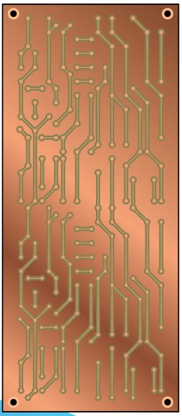
4.12 Outer Layer Imaging
An additional layer of a photoresist is smeared onto the section to replicate the outer layers of your PCB design. It usually follows the exact process similar to the previous one, and it creates a transposition of the segments inside.
4.13 Copper and Tin Plating
The additional set of the copper plating is finished, and at this moment the photoresist layers would need to be ensured that the copper would only deposit on the preferred parts on a PCB prototype board. Usually, the board gets tin plating so to safeguard the copper throughout the next stage.
4.14 Final Etching
The prototype manufacturer of PCBs is making use of chemical solutions so to get rid of any excess copper. And with the use of tin plating, the copper maintains the conductive zones protected. Then, the conductive links are done after this.
4.15 Apply Solder Mask
Rub the panel neat, then place an epoxy solder mask ink on the group. After that, you will need to display the PCB prototype board to ultraviolet light so to toughen the film. Later, detach the untoughened parts.
4.16 Apply Surface Finish
Deposit more plating, using either gold or silver to get a surface finish. The PCB prototype manufacturer might use hot air leveling to make sure the pads are consistent.
4.17 Apply Silkscreen
The silkscreen is spread throughout the surface of the printed circuit board prototype by using ink-jet writing which carries vital information concerning the board.
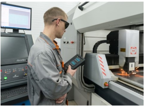
4.18 Cutting Board
After assessing out the electrical functions of your PCB prototype, the prototype manufacturer of your PCB cuts the dispersed board from a bigger panel through the use of either a router or a v-groove. And this makes it more straightforward to get the dispersed board out of the panel.
4.19 Components Sourcing
At the point where you entered and began the assembling phase of PCB prototype, you will need to gather up all the essential components. And you can attain this by yourself, or you can also seek out for help with a prototype manufacturer of PCBs. One or the other way, the bill of materials you made earlier would come in useful at this moment.
4.20 PCB Prototype Assembly
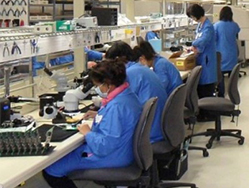
Once you gather up all the materials and components, the prototype manufacturer of your PCB will do the job of assembling them for you.
4.21 Solder Paste Stenciling
The prototype manufacturer of the PCB uses a solder paste onto the board, and this results to a blend with a flux so to assist the solder bond and melt to the PCB prototype board surface.
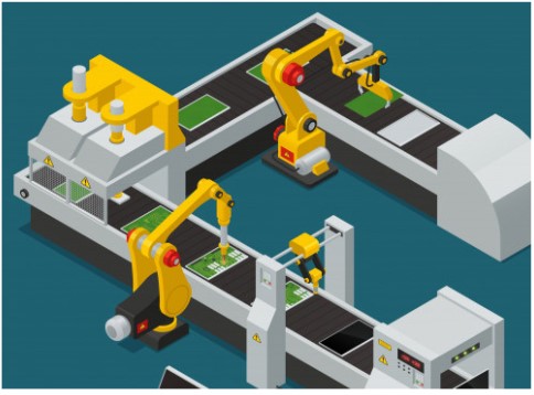
Through placing a stainless steel template on the topmost of your PCB prototype, the specific applicator can only put solder paste to the zones wherein the components will be in the finalized PCB prototype. It widens the solder paste equally to every accessible area. At the time the stainless steel template is detached, the solder paste must be put in places you want it to be left.
4.22 Picking and Placing
The prototype manufacturer of PCB will choose and put a machine to set the surface mount components (SMD) onto the PCB prototype. This device works out these components that are non-connector above the soldering paste and within areas that are preprogrammed.
4.23 Reflow Soldering
The reflow soldering stage guarantees that the solder paste is well solidified to grip all the components on the PCB prototype board.
With the use of a conveyor belt, the PCB prototype will be transported over a reflow oven within a progression of heaters to gradually warm up the board at around 480 degrees Fahrenheit, which will melt the solder within the solder paste. And as it cools down, the molten solder then solidifies, and it permanently glued the SMDs into the PCB prototype. For those PCB prototypes that have two sides or even multiple layers, reflow soldering and stenciling are performed distinctively on each layer or side.
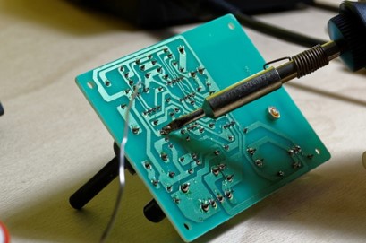
4.24 Inspecting PCB Prototype
Inspecting for some mistakes after the reflow step is essential just because there are some occasions wherein the conveyor belt produces some involuntary movements. And such changes might result in poor connection quality, electrical shortages, and even an absolute lack of connection.
X-ray inspection, Manual checks, and a programmed optical inspection are made to guarantee quality control of the PCB prototype board.
4.25 Inserting Through-Hole Components
Aside from the SMDs, some of the prototype PCB boards demands other parts such were called plated-through-hole (PTH) components. These components are plated throughout the board so to allow
them to dispatch an electrical signal coming from a side to the other.
Wave soldering or Manual soldering is essential to put in PTH components within the PCB prototype. Soldering paste will not be enough to put these components together because it’ll just only pass across the holes without holding to them. Nevertheless, wave soldering would not function well on boards that are double-sided.
4.26 Functionality Testing
The Functionality testing is at the second to the ultimate step in the process of assembling a PCB prototype. This stage imitates the typical operating situations that the PCB prototype will be exposed to.

4.27 PCB Prototype Testing
Before moving to the PCB fabrication stage or turning on your PCB prototype, circuit board manufacturing, and PCB assembly, search out for glitches in your PCB prototype board for one final time. Because it might be short circuits, populated components, routing crossovers, damaged or missing parts, inverted polarity, and many more.
Checking the PCB prototype corresponding to the intentions and goals of your project can allow you to see the flaws within the design. And if you have numerous PCB prototype boards with distinctive designs, have an identical test on them and compare the results. Afterward if possible, switch on and check the PCB prototype within the product if it will power on.
5. How to Choose a PCB Prototype Manufacturer

Are you searching for a PCB prototype manufacturer? Well, it’s not as tricky as finding a PCB assembler and manufacturer. However, most of the time, you can be able to avail on a PCB prototyping service that PCB assemblers and manufacturers offer.
More likely, select a PCB prototype manufacturer that will likewise be your final board manufacturer and assembler as well. It will save a great deal of your time instead of going back and forth to distinct service providers.
Within this chapter, we would guide you on choosing a PCB prototype manufacturer. It starts with the questions, what qualities you should be searching for? What inquiries should you be probing throughout the selection process?
We narrowed down the given criteria into eight and then discussed how they might perhaps affect your PCB prototype or the process in general.
 5.1 Cost
The cost of the production is the primary consideration for most of the companies when picking a manufacturer for a PCB prototype. If a DIY prototype PCB board or an in-house PCB prototyping is not an option, you can get in touch to a third-party which can either be a PCB manufacturer/assembler or a PCB prototype manufacturer.
A PCB manufacturer/assembler or a PCB prototype manufacturer that is located overseas could be way cheaper if you are seeking to produce PCB prototype boards for a wholesale. The price of the prototype PCB board mainly hinges on the kind of service needed as well as the expertise of the PCB prototype manufacturer.
In an instant, it might or might not cost you a great deal of money if you would impart the purchase of components to the manufacturer of the PCB prototype.
If you are asking for a price estimation from a potential PCB prototype manufacturer, you need to review and check the cited price for some hidden charges. And when you have already established a friendly relationship with the manufacturer of PCB prototype, it must not be challenging to score discounts and perks like free tooling cost, etc.
 5.2 Quality
The quality in choosing your prototype PCB boards is essential because it directly shakes up your end product’s performance as well as application.
If your prototype PCB board’s quality is already dubious at it’s testing and development stage, undoubtedly your final product will not go with what was planned. That is why a prototype PCB board must be as equally good as the finished product before it enters mass production.
One effective way to evaluate a PCB prototype manufacturer’s capabilities and performance is to observe at its product situation. And with this, you might want to ask some questions like:
- What control methods of a statistical process do a PCB manufacturer/assembler or PCB prototype manufacturer use during the PCB prototyping process?
- Does the PCB manufacturer/assembler or PCB prototype manufacturer employ a regular quality supervision improvement such as total quality management (TQM) or quality control circles (QCC)?
- Does the PCB manufacturer/assembler or PCB prototype manufacturer employ the management of engineering change order (ECO)?
- Does the PCB manufacturer/assembler or PCB prototype manufacturer adhere to the strict quality run assessments such as material inspection administration and record, equipment calibration, BOM preservation, file administration, the yield rate of SMT (surface mount technology), ESD control plan implementation, and AQL level?
 5.3 Industry Experience
PCBs are commonly used in numerous products across various industries. For this reason, it’s difficult to discover one that are masters of all and covers all the sectors.
Often, these PCB manufacturer/assembler or PCB prototype manufacturer are providing support to multiple industries but are only at a specific sector. In an instant, a PCB manufacturer/assembler or PCB prototype manufacturer for tablets and smartphones are undoubtedly good at producing prototype PCB boards that are space-constrained.
Therefore, it is so crucial to be aware of your industry well so you would recognize what qualities to search for in a PCB manufacturer/assembler or PCB prototype manufacturer. It typically makes it contracting a PCB manufacturer/assembler, or PCB prototype manufacturer that sees its capabilities at best will accelerate the PCB prototyping process, even if there are infrequent incidences of changes.
5.4 Certifications and Competencies
You can express how well-rounded and competent the PCB manufacturer/assembler or PCB prototype manufacturer through their compliances and certifications. Being well-rounded and responsible are the cornerstones of any companies favorite to manufacture high-end products.
Seek for PCB manufacturer/assembler or PCB prototype manufacturer that is UL-approved (a product that meets defined, specific requirements) , ISO 900:2008-certified (quality management system), RoHS-compliant (certified to be free from hazardous substances). Picking a PCB manufacturer/assembler or PCB prototype manufacturer that happens to meet these kinds of certifications as well as other standards, your future product, and prototype PCB boards are in reliable hands.
 5.5 Equipment
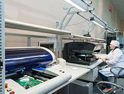
It is very crucial to grasp the list of equipment that your prospective PCB prototype manufacturer already have so that you could discern if they can meet your requirements and needs.
Take, for example, PCB designs that naturally necessitate SMT components must be done through a PCB manufacturer/assembler or PCB prototype manufacturer that has a pick-and-place equipment on its own, reflow ovens, rework tools, and 3D BGA inspectors,
Having state-of-the-art equipment alone does not determine the attribute of work to be finished. However, it is a good indicator. Hence, the material isn’t just about how fancy or costly it is. And whatever there is inside a PCB manufacturer/assembler or PCB prototype manufacturer arsenal, it should lend you even small idea on the quality of a prototype PCB board you will have and whether you will receive a timely order or not.
 5.6 Customer Service
The prototyping process of PCB might not be as hard as the PCB manufacturing or the assembly itself. However, the customer assistance from the order levels up to the production is a requirement that customers deserve. The Customer service might not look like it has a direct impact on the quality of your prototype PCB board, it surely has a massive effect on how smooth the process of your PCB prototyping is going to be.
An illustrious PCB manufacturer/assembler or a prototype manufacturer from PCB manufacturing companies assist the needs of his customers first and then offers an open line of conversation wherein they can comfortably allow their concerns. And ever since the process of negotiation began, you must be capable of telling through an email, call or text replies if a PCB prototype manufacturer can respond to you promptly.
 5.7 Minimum Order Quantity
The minimum order quantity (MOQ) differentiates on each PCB prototype manufacturer, and it largely depends on the scope and size of the product depending on the size and scope of a project. And since it’s just a PCB prototyping process, a PCB prototype manufacturer would have considered low MOQ, which might be anything from a one prototype PCB board to a dozen set of them.
 5.8 Lead Time
Lead time is essential too in the PCB prototyping process. Performing an in-house PCB prototyping lets you steer control of your operations and progress if you are capable in doing so.
And if you’re not well informed of how PCB prototyping works, search for a PCB prototype manufacturer that suggests a whole turnkey service–from the PCB prototyping and even up to PCB manufacturing/assembly–to diminish delays in the process. In such moments, you would only need to submit it to your PCB manufacturer/assembler or PCB prototype manufacturer, and they can take it from there.
 Take note, though, that the outsourced PCB prototyping whether overseas or domestically has a significant effect on the lead time. PCB manufacturer/assembler or PCB prototype manufacturer that is located overseas/abroad, especially on a China PCB manufacturer, could give you a cheaper choice. Nonetheless, if you’re pressured by a deadline, getting an overseas contracted PCB prototype manufacturer may not be a right decision. In that case, PCB prototype manufacturers that are available locally or domestically are the better option you could have.
Now, if you would like to track the lead time of your PCB manufacturing process, you will need to ensure a well-chosen PCB prototyping company that provides a service of order tracking beyond just the promise of delivering your PCB prototype boards on the scheduled time. Additionally, almost all PCB prototyping/manufacturing/assembly companies begin the work the instance the boards and parts had become available.
6. Conclusion
The PCB prototyping has been ascertained as an excellent technique to prevent PCB design fiasco in the course of mass production. And when going through the process of PCB prototyping guarantees that your PCB prototype board is prepared for takeoff before stepping up to PCB fabrication and assembly.
Before progressing to the PCB prototyping process, you will need to have your ducks in an array first. You can perform this by acquiring what Gerber files are, which PCB design software should you be using, and the PCB fabrication specs.
Whether you outsource or in-house when it comes with your PCB prototyping process, you must always weigh the pros and cons. If you like to safeguard your streamline and intellectual property, the PCB prototyping process that suits your needs is in-house. And if you would prefer to save a lot of money, then outsourcing may be the option that is apt for your needs to and to manufacture your prototype PCB board.
The PCB prototype manufacturer is similarly a key feature in the attributes of your PCB prototype; that’s why it is essential to find the right one. Within Chapter #5, we have narrowed down all the aspects that come into play when searching for a PCB prototype manufacturer that suits the bill.
When selecting a PCB prototype manufacturer and probably your PCB fabricator/assembler, note that, only you have the last call because you know the priorities and goals you have. Picking up a fitted PCB prototype manufacturer must be based on aspects like industry experience, cost, lead time, and competencies, among others.
That would be all for the PCB prototyping process. We hope you find these informative. If you have inquiries, write them in the comments below so that we can get back to you as soon as we can.






26 comments